キーワード / Keywords
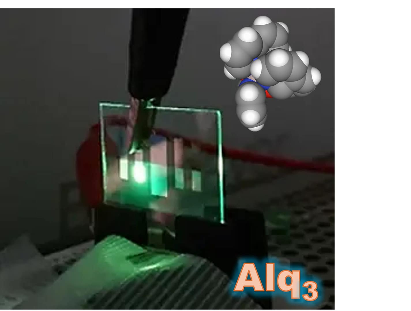
1. Alq3(トリス(8-キノリノラト)アルミニウム)
日本語:OLEDで電子輸送層や発光層に用いられる代表的な有機材料です。成膜条件によって結晶の成長や表面状態が変わり、電気特性にも影響します。
English: A representative organic semiconductor used in OLED electron-transport and emitting layers whose structure depends strongly on deposition conditions.
2. 熱蒸着(Thermal Deposition)
日本語:材料を真空中で加熱して蒸発させ、基板上に薄膜として積み重ねる方法です。基板温度や蒸着時間が膜の厚さ、結晶性、均一性を左右します。
English: A vacuum process that evaporates a heated material and deposits it as a film, with temperature and time controlling film structure.
3. 柱状成長(Columnar Growth)
日本語:結晶や粒子が基板に対して柱のように伸びる成長形態です。膜が厚くなると表面の凹凸や層間接触の不均一さにつながる場合があります。
English: A film-growth morphology in which crystalline regions extend like columns, potentially increasing roughness and contact nonuniformity.
4. 表面粗さ(Surface Roughness)
日本語:薄膜表面の凹凸の大きさを表す指標です。粗さが増すと、上に重ねる層との接触や電流分布が不均一になり、測定値にもばらつきが生じます。
English: A measure of surface height variation that can affect interlayer contact, electrical uniformity, and measurement reproducibility.
5. 電荷蓄積(Charge Accumulation)
日本語:電子や正孔が材料内部や界面の一部に偏ってたまる現象です。局所的な電場や発熱を引き起こし、OLEDの劣化や寿命低下につながる可能性があります。
English: The localized buildup of electrons or holes, which may create nonuniform fields, heating, and pathways for OLED degradation.
日本語版
研究背景
OLEDは、複数の有機薄膜を積み重ね、電子と正孔が出会うことで発光するデバイスです。その性能は、発光分子の性質だけでなく、各層の厚さ、表面の平滑さ、上下の層がどれだけ均一に接触しているかにも左右されます。特に、膜が厚くなる用途や多層構造では、成膜中に生じる微細な結晶成長が電気の流れへ影響する可能性があります。
Alq3はOLEDで広く研究されてきた有機半導体材料です。今回の研究は、熱蒸着の温度と時間を変えたとき、Alq3厚膜の結晶形態と表面状態がどのように変化し、その変化が電子輸送や積層構造へどのような影響を及ぼし得るかを調べています。
研究内容
Microstructure Evolution of Thermally Deposited Alq3 Thick Films With Deposition Temperature and Time
- 温度と蒸着時間を制御しながら、熱蒸着法でAlq3厚膜を作製しました。
- 蒸着温度と時間が増えるにつれて、Alq3は柱状に成長する形態を示しました。
- 柱状構造の発達に伴い、薄膜表面の粗さも増加しました。
- 厚さや表面形態による電気的影響を調べるため、電子だけを流す電子専用デバイスを作製しました。
- 実測した抵抗率は理論予測より高く、表面粗さによって測定値のずれも生じました。
- 粗い柱状表面は、垂直方向に積み重ねる有機層同士の接触を妨げる可能性が示されました。
- 接触の不均一さは、局所的な電荷蓄積を引き起こし、素子の劣化や動作寿命の低下につながる可能性があります。
期待される応用
この研究は、OLED材料の性能を評価するとき、化学組成だけでなく、成膜中に形成される微細構造を確認する重要性を示しています。Alq3膜が柱状に成長して表面が粗くなると、次に重ねる層との接触が場所によって異なり、電流が一部へ集中する可能性があります。したがって、基板温度、蒸着時間、膜厚を適切に管理し、平滑で均一な界面を作ることが、安定した電子輸送と長寿命化につながると考えられます。
今後は、薄膜から厚膜までの連続的な構造変化、実際の多層OLEDにおける電流分布、粗さと寿命の定量的な関係を検証することで、製造条件の最適化に役立つ可能性があります。大型ディスプレイや積層型OLEDのように、広い面積で均一性が求められるデバイスでは、材料の選択と同じくらい成膜プロセスの制御が重要になります。
English Version
Microstructural Control of Alq3 Films for More Reliable OLEDs
Research Background
OLEDs are multilayer devices in which electrons and holes travel through organic films and recombine to produce light. Their performance depends not only on the chemical properties of the emitting materials but also on film thickness, surface smoothness, and uniform contact between neighboring layers. In thick or vertically stacked structures, microstructural changes during deposition can alter charge transport and device reliability.
Alq3 is a widely studied organic semiconductor used in OLED-related layers. The featured study examined how thermal-deposition temperature and duration affect the crystal-growth morphology and surface condition of thick Alq3 films, and how these structural changes may influence electrical behavior.
Research Highlights
Microstructure Evolution of Thermally Deposited Alq3 Thick Films With Deposition Temperature and Time
- Thick Alq3 films were fabricated by thermal deposition under controlled temperature and deposition-time conditions.
- Increasing deposition temperature and time promoted a columnar growth morphology.
- Surface roughness increased as the columnar structure developed.
- Electron-only devices were prepared to assess the electrical consequences of thickness and morphology.
- Measured resistivity values were higher than theoretical predictions, and measurement deviations depended on film roughness.
- Columnar surfaces may hinder effective contact between layers in vertically stacked OLED structures.
- Morphological nonuniformity may promote localized charge accumulation, contributing to degradation and shorter operational lifetime.
Potential Applications
The results show that OLED material evaluation should consider deposited microstructure as well as chemical composition. If an Alq3 film develops a rough columnar surface, contact with the next organic layer may become spatially uneven and current may concentrate locally. Careful control of substrate temperature, deposition time, and film thickness may therefore support more uniform electron transport and improved reliability.
Future investigations could connect structural evolution across a wider thickness range with current distribution and lifetime in complete multilayer OLEDs. Such process control may be particularly important for large-area and stacked OLED devices, where uniform interfaces are essential for consistent performance.
References / 文献
- Park, G. B.; Go, B. H.; Kim, J. Y.; Shin, D. C. Microstructure Evolution of Thermally Deposited Alq3 Thick Films With Deposition Temperature and Time. Physica Status Solidi A: Applications and Materials Science 223(10) (2026), e70388. DOI: 10.1002/pssa.70388